High-irradiance, multi-wavelength, and customizable photo-curing systems engineered for precision electronics, high-speed printing, and industrial assembly.
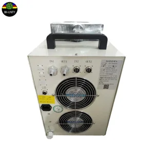
Unpacking the shift from conventional arc lamps to solid-state UV LED technology in high-performance manufacturing environments.
The global manufacturing sector is undergoing an unprecedented technological transition. Traditional mercury arc systems, which dominated the coating, bonding, and printing fields for decades, are being rapidly phased out. In their place, high-speed UV LED curing technology has emerged as the definitive standard for industrial drying and light fixing. Driven by international environmental treaties like the Minamata Convention on Mercury and the relentless demand for higher throughput, manufacturers require reliable, high-performance solid-state optoelectronics.
Integration of real-time monitoring sensors, thermal tracking, and direct feedback loops via PLC (Programmable Logic Controller) systems ensures zero-defect manufacturing.
Combining multiple wavelengths (e.g., 365nm for surface cure and 395nm for deep-layer penetration) in a single module to cure complex, thick chemistry compositions.
Pushing peak irradiances to 24W/cm² and above to keep pace with state-of-the-art flexography and offset packaging printing machinery.
An authoritative guide for global buyers and procurement directors analyzing UV LED manufacturing partners.
Procuring industrial-grade UV curing components requires a deep understanding of optoelectronic physics and thermodynamic management. A failure to assess these elements can lead to premature LED degradation, inconsistent polymerization, and expensive downtime. When evaluating a potential exporter, particularly in complex export corridors, engineering teams must evaluate three core technical markers:
| Parameter | Technical Requirement | Industrial Impact | Crucial Consideration |
|---|---|---|---|
| Peak Irradiance (W/cm²) | 10 to 24+ W/cm² measured at the exit window. | Determines the speed of photoinitiator activation on the substrate surface. | Must verify if rated at 100% duty cycle or peak transient capacity. |
| Thermal Dissipation | Microchannel water cooling or copper-fin forced air. | Controls junction temperature (Tj) to maintain optical power stability. | Water-cooled systems are mandatory for continuous line speeds above 150m/min. |
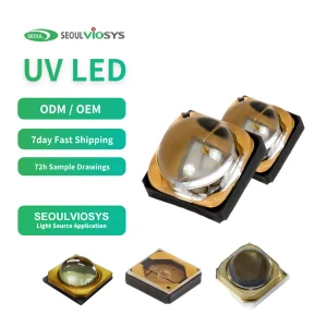
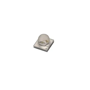
| Chip-on-Board (COB) Density | High-density SMD packaging on ceramic (AlN) substrates. | Minimizes gaps in light output, ensuring uniform curing across the entire web width. | Low-quality arrays produce "optical shadows," leading to localized sticky spots. |
| Wavelength Uniformity | Tolerance of ±5nm across the entire length of the lamp array. | Ensures consistent curing depth and chemical cross-linking. | Poor bins lead to uneven adhesion, peeling, and color shifts. |
Furthermore, the physical build quality of the curing chamber and module must withstand hostile environments characterized by airborne dust, vaporized inks, and mechanical vibrations. Systems featuring automated shutter mechanisms, ozone-free emissions, and integrated quartz protection windows are highly preferred in heavy industrial environments like metal decorating and high-speed packaging lines.
A deep dive into one of China's premier developers and manufacturers of customized industrial UV LED systems.
Dongguan LumiCure Light Co., Ltd. is a professional China UV LED curing lamp manufacturer specializing in the research, development, production, and supply of industrial UV curing systems and customized UV LED solutions. With a strong focus on innovation, quality, and customer satisfaction, LumiCure has become a trusted partner for manufacturers worldwide seeking efficient and reliable curing technologies.
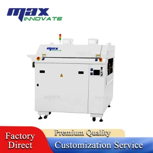
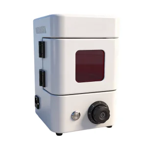
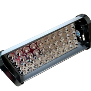
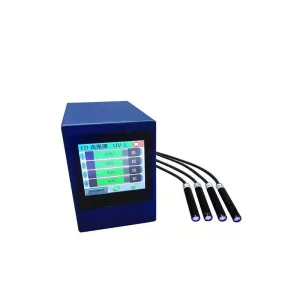
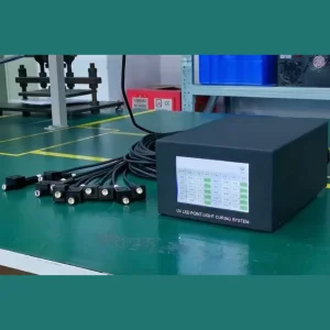
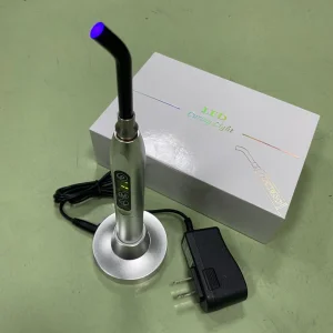
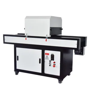
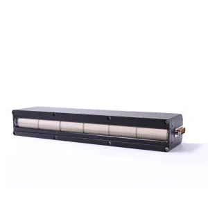
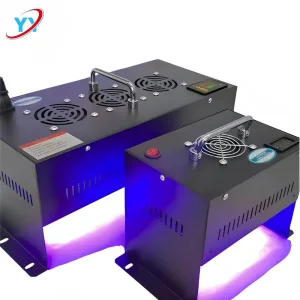
Our product range includes UV LED curing lamps, UV LED spot curing systems, flood curing lamps, conveyor UV curing machines, UV LED modules, printing curing systems, adhesive curing equipment, and customized industrial UV solutions. These products are widely applied in printing, electronics assembly, semiconductor packaging, optical bonding, automotive manufacturing, medical devices, 3D printing, and various precision industrial processes.
Backed by an experienced engineering team and advanced manufacturing facilities, LumiCure is committed to developing energy-saving and environmentally friendly UV curing technologies. Our products feature high curing efficiency, precise wavelength output, long service life, low maintenance requirements, and intelligent control capabilities, helping customers improve productivity while reducing operating costs.
Quality remains the foundation of our business. Every product undergoes rigorous testing and strict quality control procedures throughout the manufacturing process to ensure consistent performance and reliability. We also provide comprehensive OEM and ODM services, enabling customers to customize products according to their specific technical and application requirements.
Serving clients across Europe, North America, Asia, the Middle East, and other global markets, Dongguan LumiCure Light Co., Ltd. continues to deliver innovative UV LED curing solutions that support sustainable and efficient industrial manufacturing.
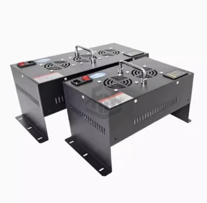
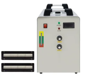
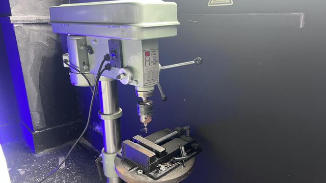
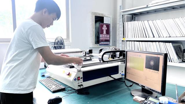
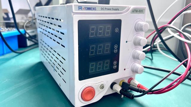
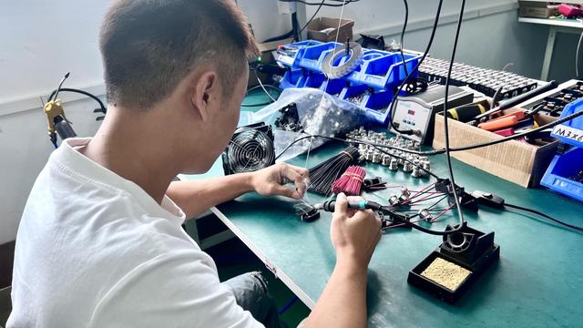
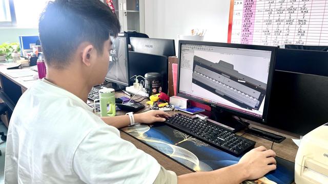
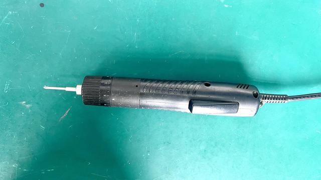
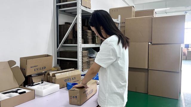
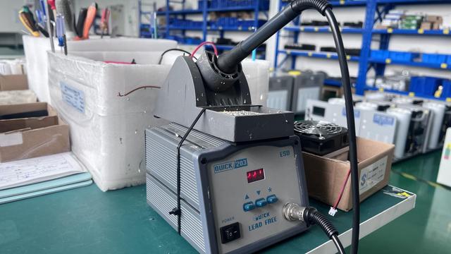
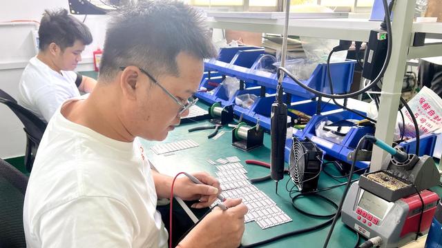
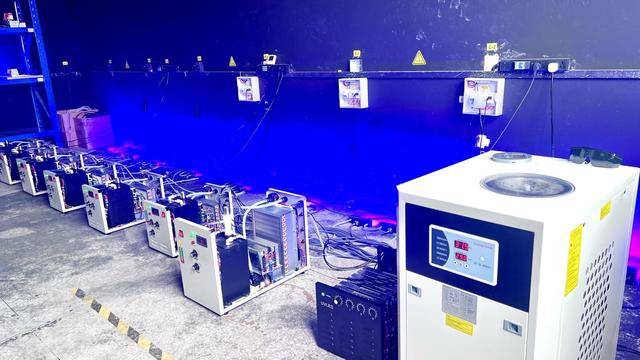
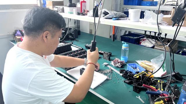
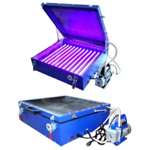
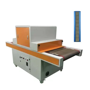
LumiCure's success is rooted in its capability to translate complex optoelectronic parameters into functional, high-yield manufacturing tools. Whether a client requires low-intensity spot-curing for medical catheter assembly or ultra-high-power modules for roll-fed offset presses, the integration of premium raw material inputs (high-quality chip arrays, proprietary thermal compound layers, and high-performance drivers) assures consistent energy output. The following photo gallery exhibits LumiCure's advanced design, cleanroom production lines, and customized machinery setups:
Why leading global manufacturers consolidate their custom UV LED sourcing in China's advanced industrial hubs.
The manufacturing ecosystem in Southern China, specifically centered in Shenzhen and Dongguan, has matured beyond pure labor-cost advantages. Today, it represents the world's most dense cluster of optoelectronic engineering capability. "Factory 4.0" is not merely about robotics; it is the tight horizontal integration of optical simulation labs, precision CNC housing fabricators, advanced semiconductor packaging facilities, and automated testing hubs within a 50-kilometer radius.
For international buyers looking to secure high-speed UV LED curing modules, this localization translates directly into rapid iteration cycles. A custom optical lens layout designed to eliminate light divergence on a specific printing line can be simulated, prototyped, machined, and mounted on a testbench within five business days. The comparative lead time in traditional Western manufacturing ecosystems is often four to six weeks.
This agility is further backed by rigid compliance frameworks. Major exporters maintain ISO 9001:2015 registries and implement optical power calibrators calibrated to NIST standards, ensuring that a system shipped to Germany, the US, or Japan delivers exactly the irradiance specified in the datasheet.
Detailed examination of how UV LED curing interfaces with real-world production challenges.
Modern PCBs require precise application of conformal coatings, dam-and-fill encapsulants, and optical display bonding glues. Traditional heat curing threatens heat-sensitive microprocessors. High-intensity 365nm spot or flood curing systems cure shadowless UV adhesives in under 2 seconds, ensuring zero component migration on high-speed SMT assembly lines.
In narrow and wide-web label printing, printing speeds often exceed 200 meters per minute. Curing must occur instantaneously to prevent color bleed and maintain crisp text down to 2-point sizes. UV LED lamp arrays integrated directly onto offset and flexographic printing stations supply intense energy outputs, enabling immediate rewinding and post-press processing.
For items like needles, syringes, catheters, and IV tubes, material integrity is life-critical. UV curing is highly prized because it produces clean, non-toxic, and chemical-resistant bonds. Micro-spot systems running at 365nm focus high energy densities precisely on the joint, avoiding thermal exposure to delicate plastic components.
Technical insights addressing key questions from optoelectronic engineers and global procurement managers.
Explore our specialized, high-power systems designed for heavy industrial configurations and continuous operation.
 LumiCure Light